Basic methods of studying nanostructured materials.
Objectives:
Ø To describe how to characterize nanomaterials.
Observation is the key to making new discoveries, and this is impossible on the nanoscale, at a glance. In recent years, new techniques have been developed that complement and surpass the performance of the instruments so far used in the study of matter at the atomic and molecular scales.
The new techniques available open the doors to a more precise knowledge of the nanostructure of matter and the manufacture of nanostructured materials.
The key parameters of nanoparticle’s physical characterization include, size, shape, surface, and the morphology. For example, size is one of the principle properties of nanoparticles, which are related to the surface to volume ratio. The chemical composition is important. In general, there are several techniques to evaluate the physical and chemical characterizations of nanoparticles.
1. Electronic Microscopy
Electron microscopy uses a beam of accelerated electrons to provide a much higher resolution, which cannot be achieved by light microscope. The most commonly used are transmission electron microscopy (TEM) and scanning electron microscopy (SEM).
1.1. Transmission electron microscope (TEM) is the most widely used characterization tool to determine the shape and size of nanoparticles (Fig. 1) Although there are other methods, such as dynamic light scattering (DSL) and scattering of small-angle X-rays (SAXS), which can be used to measure the size of particles, the TEM is the only one that gives us real images of the shapes of the nanostructures.
The preparation of the sample of a colloidal suspension for TEM is quite simple, which consists of depositing a drop of the colloidal suspension on the copper grid for TEM coated with carbon, and allowing the evaporation of the solvent, preferably in a vacuum chamber.
The TEM uses a high voltage electron beam to illuminate the specimen and generate an image. The electron beam is originated from an electron gun, accelerated and then transmitted through the specimen on a conducting grid. The transmitted electron carries information about the structure of the specimen, and such information can be recorded by an imaging detector (fluorescence screen or CCD camera). The TEM normally requires extremely thin section of specimen, typically no more than 100 nm. This is one of the major disadvantages of the transmission electron microscope.
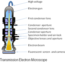
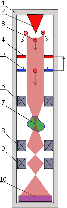
Fig. 1. Transmission electron microscope. (1) case, (2) electron emitter, (3) electrons, (4) cathode, (5) anode, (6) condenser lens, (7) sample analyzed, (8) objective lens, (9) projector lens, (10) Detector (sensor or photographic film).
1.2. The scanning electron microscope (SEM) is an instrument that allows the observation and surface characterization of inorganic and organic materials, providing morphological information of the material analyzed (Fig. 2 and 3).
The main utilities of the SEM are the high resolution (~ 100 Å), the great depth of field that gives three-dimensional appearance to the images and the simple preparation of the samples.
The SEM is based on the interaction of the electron beam with the specimen surface. Due to the high depth of field in SEM, a three-dimensional appearance can be displayed. If not conductive, the specimen needs to be coated with an ultrathin layer of conductive material like gold, platinum or graphite to obtain a clear image. The substrate, where the specimen is held, is typically a filter membrane or a conducting grid.
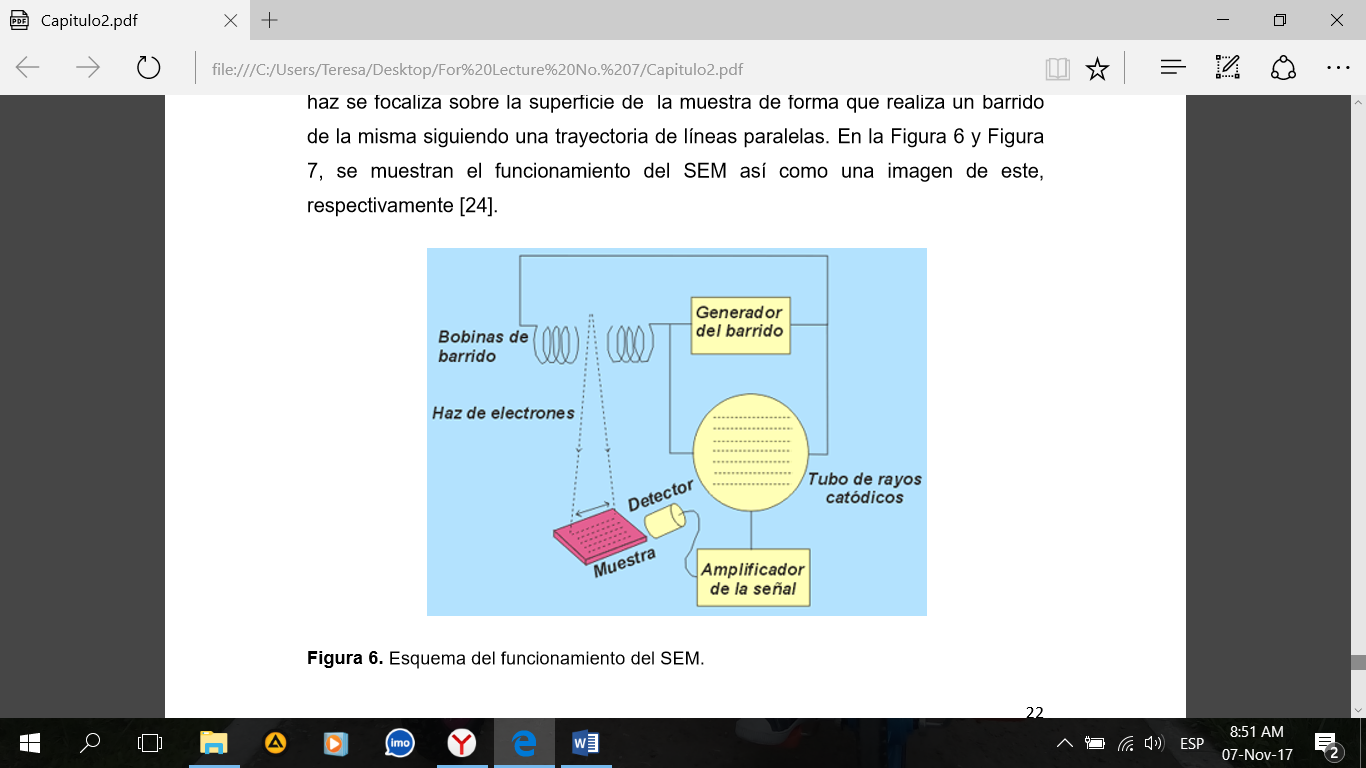
Figure 2. Schematic of the SEM operation.
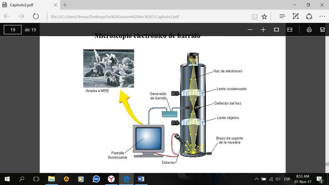
Figure 3. Scanning electron microscope (SEM).
2. Spectral methods of research.
Spectral methods usually include methods for studying the surface of solids, based on an analysis of the energy spectra of the reflected radiations arising from irradiation of the studied material by electrons, ions, and photons
2.1. Electronic Auger Spectroscopy (AES)
Auger electron spectroscopy is a common analytical technique used specifically in the study of surfaces and, more generally, in materials science. This method is based on the energy analysis of secondary Auger electrons. The Auger effect is named after the French physicist who discovered it in 1925. The falling electron is knocking out the electron of the inner shell of the atom. Because of the excitation of atoms, secondary electron emission is observed on the surface of the sample. A small fraction of them (of the order of 10-5) leaves the sample because of inter-orbital transitions without simultaneous emission of photons (X-ray quanta). Such electrons are called Auger electrons. The kinetic energy of the Auger electron is determined by the difference in the energies of the inner shell with which the electron was knocked out and by the energy of the higher-lying energy level, from where the electron with the Auger electron ejection passes to the vacancy formed. On the energy of Auger electrons, one can judge the properties of the atoms that emitted them. Thus, an analysis of the energy spectra of Auger electrons allows us to judge the chemical composition of the surface layer of the substance under study, and in a number of cases also provides information on the chemical bonds of the atoms in it. It is possible to determine all the elements heavier than helium. In devices that realize electron Auger spectroscopy, the energy of electrons in the incident beam is 0.1-3 keV. In this case, the composition of the surface at a depth of 0.5-3.0 nm is investigated. The main contribution to the signal is made by the first two or three layers of atoms. The resolution on the surface is determined by the diameter of the primary electron beam and is up to 50 nm.
2.2. Secondary ion mass spectroscopy
It is a technique used to analyze the composition of solid surfaces and thin films by sputtering the surface of the specimen with an ion beam and collecting and analyzing ejected secondary ions. Secondary ions carry information about the chemical composition of 2-3 surface atomic layers in the probe zone and are investigated by means of a mass spectrometer. The method has a high sensitivity and allows determining all chemical elements, including hydrogen and helium.
2.3. Laser microprobe analysis
It is a mass spectrometer that uses a focused laser for microanalysis. It employs local ionization by a pulsed laser and subsequent mass analysis of the generated ions. In laser microprobe mass analysis, a highly-focused laser beam is pulsed on a micro sample usually with a volume of approximately 1 microliter. The resulting ions generated by this laser are then analyzed with mass spectrometry to give composition, concentration, and in the case of organic molecules structural information.
The disadvantage of the method is a rather low accuracy in determining the quantitative content of elements (for basic elements, the error is up to 10%, and for elements present in a very small number - up to 30%).
3. Scanning Probe Test Methods
This group of methods is the most widely used in the field of nanomaterials and nanotechnologies. The main idea of all methods of this group is to use a probe - a device for reading information from the surface of the material being studied. In most cases, a diamond needle with a tip radius of about 10 nm is used as the working body of the probe. Using a high-precision positioning (scanning) mechanism, the probe is moved over the surface of the sample in three coordinates. Typically, there is a range of displacement of the probe: coarse movement with relatively low accuracy and high speed and accurate movement with a sufficiently low speed and high positioning accuracy to 0.1-1 nm. A greater accuracy of positioning is provided as a rule in height. The signal from the probe is processed by a computer and converted into a three-dimensional image. To process the signals to be removed, filter and correct them, special software packages are used. The cost and size of probe microscopes are usually much lower than those of electronic microscopes, and the possibilities are quite commensurable. Moreover, for a number of probe microscopy options, the presence of vacuum is not required, research materials can be very diverse, including insulators, semiconductors, biological objects. In this case, studies can be conducted without significant damage to the object and with a fairly simple preparation of its surface (for example, only polishing a separate section).
3.1. Scanning tunneling microscope (STM)
In this method, an electrically conducting tip is used as the probe (Figure 4). A voltage of the order of 01-10 V is created between the probe and the sample. A tunnel current of about 1-10 nA arises in the gap, which depends on the properties and configuration of the atoms on the material surface under study. This current is recorded by the instruments. Tunneling this method is called in connection with the fact that the current arises from the tunnel effect, namely the quantum transition of an electron through a region forbidden by classical mechanics. This area is a gap of 2-10 Å between the tip of the needle and the nearest point of the surface of the material being studied. The energy of the tunneling electrons is of the order of 1 eV. In modern devices, a mode is realized in which the value of the tunnel current is maintained constant due to the instrumental implementation of the feedback, which changes the gap (by moving the probe along the Z axis). Under the most favorable conditions, the method of scanning tunneling microscopy provides a resolution in the plane (x and y coordinates) to 1 Å, and in height (coordinate z) - up to 0.01 Å. There are many options for upgrading and supplementing this method. So scanning tunnel spectroscopy is based on the analysis of current-voltage characteristics at different points of the surface or the obtaining of surface images at different voltages. In the first case, it is possible to determine the type of atom over which the needle stopped over the value of the second derivative of the tunnel current, and in the second case to determine the parameters of the band structure for semiconductors and superconductors.
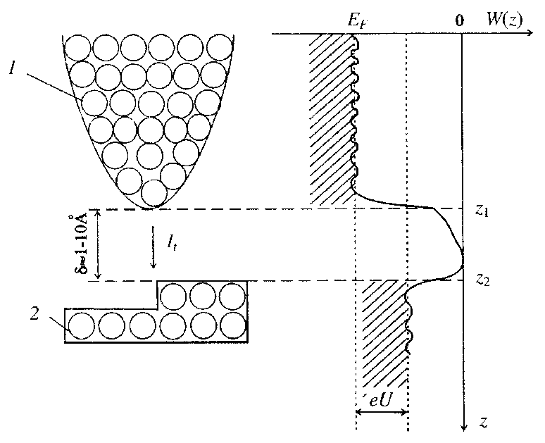
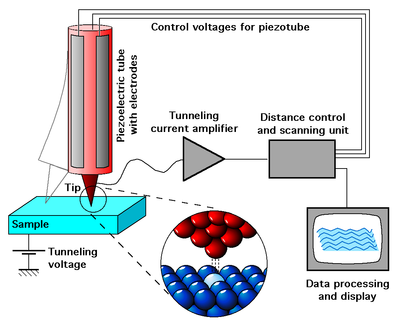
Fig.4. Schematic diagram of the scanning tunneling microscope: 1- probe, 2-sample, It is the tunnel current in the gap, δ, EF is the Fermi level, U is the voltage applied between the probe and the sample, W is the energy, e is the electron charge, Z - axis of coordinates in height.
The limitations of the scanning tunneling microscopy method are the mandatory conductivity of the sample material and the need for high or ultrahigh vacuum and low temperatures (up to 50-100 K) to obtain high resolutions. At the same time, for resolution within the range of about 1 nm these requirements are not necessary.
3.2. Atomic Force Microscopy (AFM)
In this method, the change in the interaction force between the tip of the probe (needle) and the surface under investigation is recorded. The needle is located on the end of a cantilevered beam of known rigidity, capable of bending under the action of small forces arising between the sample surface and the tip of the tip (Figure 5).
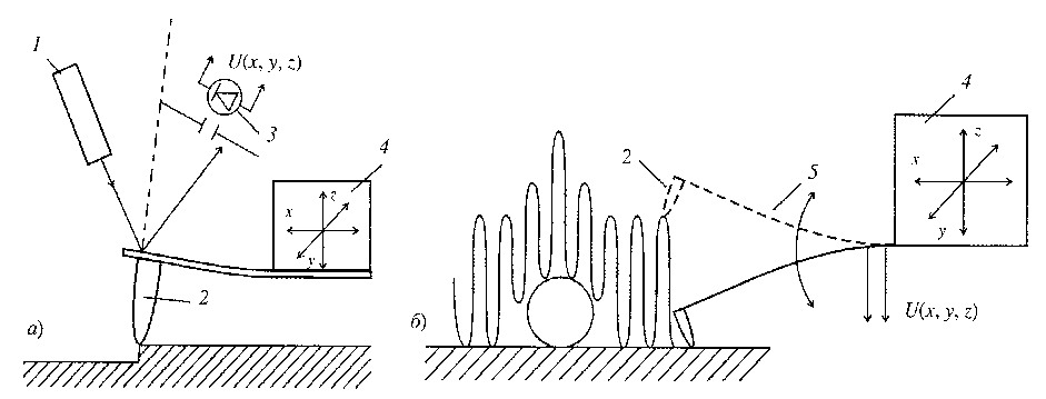
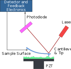
Fig. 5. Schemes of two modes of the method of atomic force microscopy: a) contact mode, b) quasi-contact mode: 1- laser, 2- needle, 3- cantilever deflection or vibration measuring system, 4- force registration system acting on the needle.
These forces in a number of variants of the method can be van der Waals (molecular), electrostatic or magnetic. A needle with a needle is called a cantilever. The deformation of the cantilever is measured by the deflection of the laser beam incident on its rear surface, or by the piezo resistive effect that occurs in the cantilever material during bending.
There are two modes of the atomic-force microscopy method. With the contact mode, the tip of the needle (diamond, fullerite or silicon with a hardening coating) is in continuous operation in contact with the surface under investigation. At simplicity of realization of this mode there is also a disadvantage - the possibility of damage to the material or needle being examined. In "quasi-contact" or "non-contact" mode, the parameters of the cantilever's natural oscillations (resonance frequencies, damping of oscillations, phase shift between the acting force and displacement) are measured. The cantilever needle is in this case at a certain distance from the sample surface (10-500 Å) and interacts with it by relatively long-range Van der Waals forces.
In a number of modern instruments, it is possible to measure the friction forces of the needle, to remove the elasticity maps of the studied sections of the material, the electric impedance, to test Nano hardness by scratching, and when using semiconductor diamond needles, the capacity of the sample surface, the conductivity of the near-surface layer, and the determination of the impurity concentration by the change in capacitance. The resolution along the plane (the x and y coordinates) is of the order of 1 nm, and the height (coordinate z) is up to 0.1 nm. The bottleneck of the method is the resistance of the needle material. However, for most of the materials studied, the hardness of a diamond or fullerite needle is quite sufficient.
There are other techniques that can be used in the characterization of nanomaterials:
ü X-Ray Diffraction (XRD)
ü Dynamic light scattering (DLS)
ü Nanoparticle Surface Area Monitor (NSAM)
ü Condensation Particle Counter (CPC)
ü Differential Mobility Analyzer
ü Scanning Mobility Particle Sizer (SMPS)
Control questions:
1. What are the key parameters in the physical characterization of nanostructured materials?
2. Describe the operating principle of the electronic scanning microscope.
3. Explain the importance of the use of Secondary ion mass spectroscopy.
4. Why the Scanning Probe Test Methods are the most widely used in the field of nanomaterials and nanotechnologies?
| <== предыдущая лекция | | | следующая лекция ==> |
| Несобственный интеграл второго рода и его вычисление. | | | Formation and development of Nanochemistry |
Дата добавления: 2018-11-25; просмотров: 1268;